- 您现在的位置:买卖IC网 > Sheet目录362800 > EVAL-AD5379EB (Analog Devices, Inc.) 40-Channel, 14-Bit, Parallel and Serial Input, Bipolar Voltage-Output DAC
AD5379
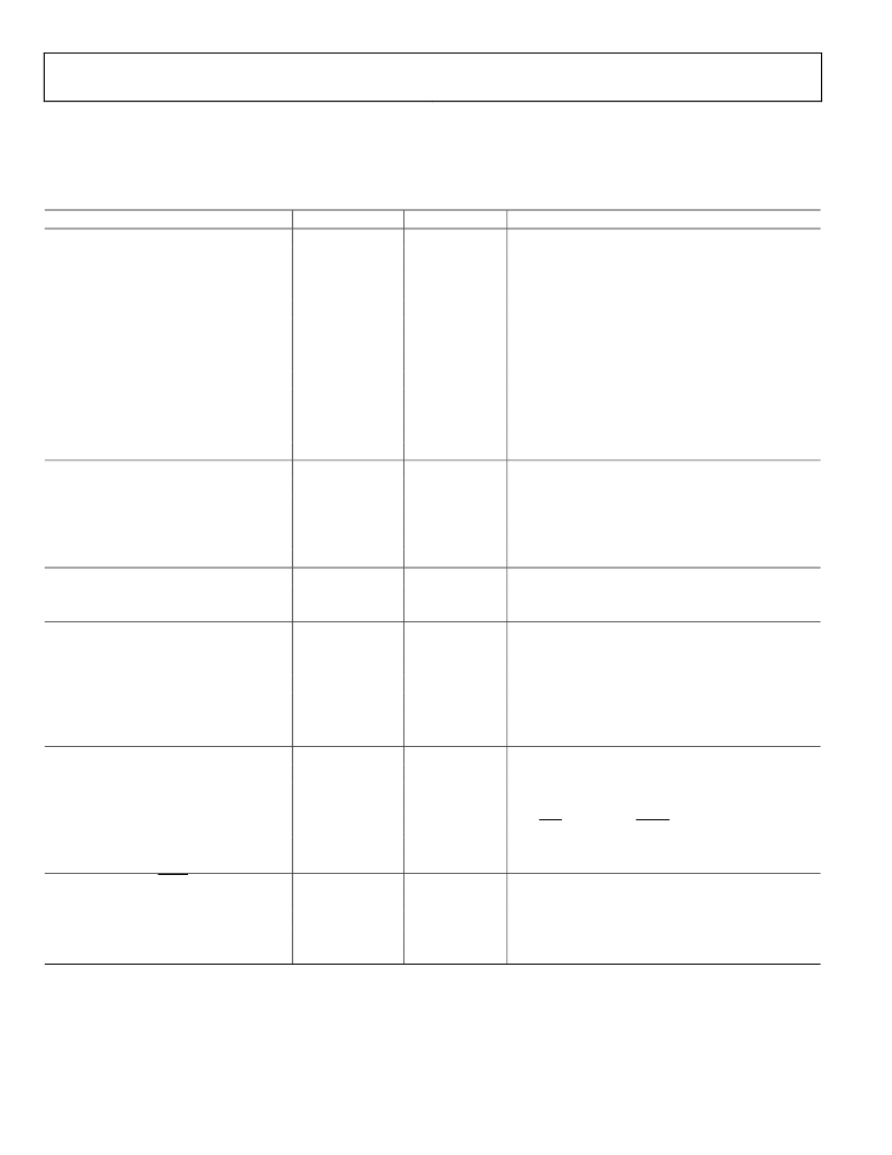
SPECIFICATIONS
V
CC
= 2.7 V to 5.5 V; V
DD
= 11.4 V to 16.5 V; V
SS
= 11.4 V to 16.5 V; V
REF
(+) = 5 V; V
REF
() = 3.5 V; AGND = DGND = REFGND = 0 V;
V
BIAS
= 5 V; C
L
= 200 pF to GND; R
L
= 11 k to 3 V; gain = 1; offset = 0 V; all specifications T
MIN
to T
MAX
, unless otherwise noted.
Table 2.
Parameter
A Version
1
Unit
ACCURACY
Resolution
14
Bits
Relative Accuracy
±3
LSB max
±2.5
LSB max
Differential Nonlinearity
1/+1.5
LSB max
Zero-Scale Error
±12
mV max
±5
mV max
Full-Scale Error
±12
mV max
±8
mV max
Gain Error
±8
mV max
±1/±5
mV typ/max
VOUT Temperature Coefficient
5
ppm FSR/°C typ
DC Crosstalk
2
0.5
mV max
REFERENCE INPUTS
2
V
REF
(+) DC Input Impedance
1
M min
V
REF
() DC Input Impedance
8
k min
V
REF
(+) Input Current
±10
μA max
V
REF
(+) Range
1.5/5
V min/max
V
REF
() Range
3.5/0
V min/max
REFGND INPUTS
2
DC Input Impedance
80
k min
Input Range
±0.5
V min/max
OUTPUT CHARACTERISTICS
2
Output Voltage Range
V
SS
+ 2/ V
SS
+ 2.5
V min
V
DD
2/ V
DD
2.5
V max
Short Circuit Current
15
mA max
Load Current
±1.5
mA max
Capacitive Load
2200
pF max
DC Output Impedance
1
max
DIGITAL INPUTS
Input High Voltage
1.7
V min
2.0
V min
Input Low Voltage
0.8
V max
Input Current (with pull-up/pull-down)
±8
μA max
Input Current (no pull-up/pull-down)
±1
μA max
Input Capacitance
2
10
pF max
DIGITAL OUTPUTS (BUSY, SDO)
Output Low Voltage
0.5
V max
Output High Voltage (SDO)
V
CC
0.5
V min
High Impedance Leakage Current
70
μA max
High Impedance Output Capacitance
2
10
pF typ
Rev. 0 | Page 4 of 28
Test Conditions/Comments
2
40°C to +85°C.
0°C to 70°C.
Guaranteed monotonic by design over temperature.
40°C to +85°C.
0°C to 70°C.
40°C to +85°C.
0°C to 70°C.
40°C to +85°C.
0°C to 70°C.
Includes linearity, offset, and gain drift. See Figure 11.
Typically 100 μV.
Typically 100 M.
Typically 12 k.
Per input. Typically ±30 nA.
±2% for specified operation.
±2% for specified operation.
Typically 120 k.
I
LOAD
= ±0.5 mA/ ±1.5 mA.
I
LOAD
= ±0.5 mA/ ±1.5 mA.
JEDEC compliant.
V
CC
= 2.7 V to 3.6 V.
V
CC
= 3.6 V to 5.5 V.
V
CC
= 2.7 V to 5.5 V.
SER/PAR, FIFOEN, and RESET pins only.
All other digital input pins.
Sinking 200 μA.
Sourcing 200 μA.
SDO only.
发布紧急采购,3分钟左右您将得到回复。
相关PDF资料
EVAL-AD5381EB
40-Channel, 3 V/5 V, Single-Supply, 12-Bit, Voltage Output DAC
EVAL-AD5382EB
32-Channel, 3 V/5 V, Single-Supply, 14-Bit, Voltage Output DAC
EVAL-AD5383EB
32-Channel, 3 V/5 V, Single-Supply, 12-Bit, Voltage Output DAC
EVAL-AD5398EB
120 mA, Current Sinking, 10-Bit, I2C DAC
EVAL-AD5415EB
Dual 12-Bit, High Bandwidth, Multiplying DAC with 4-Quadrant Resistors and Serial Interface
EVAL-AD5426EB
8-/10-/12-Bit High Bandwidth Multiplying DACs with Serial Interface
EVAL-AD5432EB
CAP, .22UF, 10V, SMT, 0603
EVAL-AD5443EB
CAP X7R 470PF 50V 10% 0603
相关代理商/技术参数
EVAL-AD5379EBZ
功能描述:BOARD EVALUATION FOR AD5379 RoHS:是 类别:编程器,开发系统 >> 评估板 - 数模转换器 (DAC) 系列:- 产品培训模块:Lead (SnPb) Finish for COTS
Obsolescence Mitigation Program 标准包装:1 系列:- DAC 的数量:4 位数:12 采样率(每秒):- 数据接口:串行,SPI? 设置时间:3µs DAC 型:电流/电压 工作温度:-40°C ~ 85°C 已供物品:板 已用 IC / 零件:MAX5581
EVAL-AD5380EB
制造商:Analog Devices 功能描述:EVALUATION BOARD I.C. - Bulk
EVAL-AD5380EBZ
功能描述:BOARD EVAL FOR AD5380 RoHS:是 类别:编程器,开发系统 >> 评估板 - 数模转换器 (DAC) 系列:- 产品培训模块:Lead (SnPb) Finish for COTS
Obsolescence Mitigation Program 标准包装:1 系列:- DAC 的数量:4 位数:12 采样率(每秒):- 数据接口:串行,SPI? 设置时间:3µs DAC 型:电流/电压 工作温度:-40°C ~ 85°C 已供物品:板 已用 IC / 零件:MAX5581
EVAL-AD5381EB
制造商:Analog Devices 功能描述:EVAL KIT FOR 40-CH, 3V/5 V, SGL-SUPPLY, 12-BIT, VOLT OUTPUT - Bulk 制造商:Rochester Electronics LLC 功能描述:
EVAL-AD5382EB
制造商:Analog Devices 功能描述:EVALUATION BOARD I.C. - Bulk 制造商:Rochester Electronics LLC 功能描述:
EVAL-AD5382EBZ
功能描述:BOARD EVAL FOR AD5382 RoHS:是 类别:编程器,开发系统 >> 评估板 - 数模转换器 (DAC) 系列:- 产品培训模块:Lead (SnPb) Finish for COTS
Obsolescence Mitigation Program 标准包装:1 系列:- DAC 的数量:4 位数:12 采样率(每秒):- 数据接口:串行,SPI? 设置时间:3µs DAC 型:电流/电压 工作温度:-40°C ~ 85°C 已供物品:板 已用 IC / 零件:MAX5581
EVAL-AD5383EB
制造商:Analog Devices 功能描述:EVAL KIT FOR 32CH, 3V/5 V, SGL-SUPPLY, 12-BIT, VOLT OUTPUT D - Bulk 制造商:Rochester Electronics LLC 功能描述:
EVAL-AD5390EB
制造商:Analog Devices 功能描述: